ATR statistics: TA1 - Global, encodes Fi and Di
Article from the series "ATR statistics"
TA1 - Global, encodes Fi and Di
The ISO 7816-3 specification is not public. So I can't copy/paste part of the text. I will use Wikipedia instead.From Wikipedia https://en.wikipedia.org/wiki/Answer_to_reset#Interface_byte_TA1 (with some edition to remove extra details):
Interface byte TA1, if present, is global, and encodes the maximum clock frequency fmax supported by the card, and the number of clock periods per ETU that it suggests to use after the ATR, expressed as the ratio Fi/Di of two integers. When TA1 is absent, it's assumed default value is ‘11’, corresponding to fmax = 5 MHz, Fi = 372, Di = 1.
The 4 low-order bits of TA1 (4th MSbit to 1st LSbit) encode Di as:
4th to 1st bits 0000 0001 0010 0011 0100 0101 0110 0111 1000 1001 1010 1011 1100 1101 1110 1111 Di RFU 1 2 4 8 16 32 64 12 20 RFU RFU RFU RFU RFU RFU
The 4 high-order bits of TA1 (8th MSbit to 5th LSbit) encode fmax and Fi as:
8th to 5th bits 0000 0001 0010 0011 0100 0101 0110 0111 1000 1001 1010 1011 1100 1101 1110 1111 Fi 372 372 558 744 1 116 1 488 1 860 RFU RFU 512 768 1 024 1 536 2 048 RFU RFU fmax (MHz) 4 5 6 8 12 16 20 — — 5 7.5 10 15 20 — —
| TA1 | # | % |
|---|---|---|
| 932 | 44.98 % | |
| 0x18 | 241 | 11.63 % |
| 0x96 | 202 | 9.75 % |
| 0x94 | 167 | 8.06 % |
| 0x95 | 158 | 7.63 % |
| 0x13 | 136 | 6.56 % |
| 0x11 | 124 | 5.98 % |
| 0x00 | 18 | 0.87 % |
| 0x91 | 16 | 0.77 % |
| 0x12 | 15 | 0.72 % |
| 0x98 | 15 | 0.72 % |
| 0x14 | 14 | 0.68 % |
| 0x21 | 8 | 0.39 % |
| 0x15 | 7 | 0.34 % |
| 0x97 | 6 | 0.29 % |
| 0x38 | 4 | 0.19 % |
| 0x01 | 1 | 0.05 % |
| 0x04 | 1 | 0.05 % |
| 0x16 | 1 | 0.05 % |
| 0x32 | 1 | 0.05 % |
| 0x36 | 1 | 0.05 % |
| 0x3F | 1 | 0.05 % |
| 0xA8 | 1 | 0.05 % |
| 0xD6 | 1 | 0.05 % |
| 0xFF | 1 | 0.05 % |

The TA1 value indicates the maximal communication speed between the card and the reader supported by the card. The reader may not support such a high speed. A lower speed will then be used (negotiated by the reader itself or by the reader driver).
Data rate (communication speed)
To know the speed value we need to convert the TA1 value in Fi/Di into a speed value in bit/s.| TA1 | Fi | Di | cycles/ETU | bits/s at 4 Mhz | Fmax Mhz | bits/s at Fmax |
|---|---|---|---|---|---|---|
| 0x01 | 372 | 1 | 372 | 10752 | 4 | 10752 |
| 0x04 | 372 | 8 | 46 | 86956 | 4 | 86956 |
| 0x16 | 372 | 32 | 11 | 363636 | 5 | 454545 |
| 0x32 | 744 | 2 | 372 | 10752 | 8 | 21505 |
| 0x36 | 744 | 32 | 23 | 173913 | 8 | 347826 |
| 0x3F | 744 | RFU | RFU | RFU | RFU | RFU |
| 0xA8 | 768 | 12 | 64 | 62500 | 7.5 | 117187.5 |
| 0xD6 | 2048 | 32 | 64 | 62500 | 20 | 312500 |
| 0xFF | RFU | RFU | RFU | RFU | RFU | RFU |
| 0x38 | 744 | 12 | 62 | 64516 | 8 | 129032 |
| 0x97 | 512 | 64 | 8 | 500000 | 5 | 625000 |
| 0x15 | 372 | 16 | 23 | 173913 | 5 | 217391 |
| 0x21 | 558 | 1 | 558 | 7168 | 6 | 10752 |
| 0x14 | 372 | 8 | 46 | 86956 | 5 | 108695 |
| 0x12 | 372 | 2 | 186 | 21505 | 5 | 26881 |
| 0x98 | 512 | 12 | 42 | 95238 | 5 | 119047 |
| 0x91 | 512 | 1 | 512 | 7812 | 5 | 9765 |
| 0x00 | 372 | RFU | RFU | RFU | RFU | RFU |
| 0x11 | 372 | 1 | 372 | 10752 | 5 | 13440 |
| 0x13 | 372 | 4 | 93 | 43010 | 5 | 53763 |
| 0x95 | 512 | 16 | 32 | 125000 | 5 | 156250 |
| 0x94 | 512 | 8 | 64 | 62500 | 5 | 78125 |
| 0x96 | 512 | 32 | 16 | 250000 | 5 | 312500 |
| 0x18 | 372 | 12 | 31 | 129032 | 5 | 161290 |
| 0x11 | 372 | 1 | 372 | 10752 | 5 | 13440 |
The table provides the data rate value for a clock of 4 Mhz. We have seen in "CCID descriptor statistics: dwDefaultClock" that 4 Mhz is the default clock of 48% of the CCID readers in my list.
You can note that there is different values of Fi and Di that give the same data rate. For example TA1=0xA8 and TA1=0xD6 both give a data rate of 62500 bits/s when using a clock at 4 MHz.
Population
We can count the number of ATR for each value of TA1. We get the table bellow:| TA1 | bits/s at 4 Mhz | bits/s at Fmax | # |
|---|---|---|---|
| 0x01 | 10752 | 10752 | 1 |
| 0x04 | 86956 | 86956 | 1 |
| 0x16 | 363636 | 454545 | 1 |
| 0x32 | 10752 | 21505 | 1 |
| 0x36 | 173913 | 347826 | 1 |
| 0x3F | RFU | RFU | 1 |
| 0xA8 | 62500 | 117187.5 | 1 |
| 0xD6 | 62500 | 312500 | 1 |
| 0xFF | RFU | RFU | 1 |
| 0x38 | 64516 | 129032 | 4 |
| 0x97 | 500000 | 625000 | 6 |
| 0x15 | 173913 | 217391 | 7 |
| 0x21 | 7168 | 10752 | 8 |
| 0x14 | 86956 | 108695 | 14 |
| 0x12 | 21505 | 26881 | 15 |
| 0x98 | 95238 | 119047 | 15 |
| 0x91 | 7812 | 9765 | 16 |
| 0x00 | RFU | RFU | 18 |
| 0x11 | 10752 | 13440 | 124 |
| 0x13 | 43010 | 53763 | 136 |
| 0x95 | 125000 | 156250 | 158 |
| 0x94 | 62500 | 78125 | 167 |
| 0x96 | 250000 | 312500 | 202 |
| 0x18 | 129032 | 161290 | 241 |
| 10752 | 13440 | 932 |
We can draw a graph of the number of ATR for a given data rates to get an idea of the repartition:
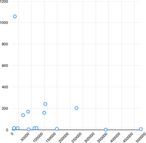
In the graph I merged the results for a same data rate. So for the value 10 752 bits/s we get the sum of TA1=0x11 and no TA1 so the default value of 0x11. The total is then 932+124=1056.
We can also compute and display the median value:
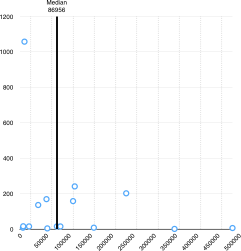
Half of the cards have a data rate below 86 956 bits/s and the other half has a data rate above 86 956 bits/s.
Using Fmax
The Fi value also gives the maximal clock speed supported by the smart card. The value goes from 4 Mhz to 20 MHz. If we reuse the same examples the maximal clock speed for TA1=0xA8 is 7.5 Mhz and for TA1=0xD6 it is 20 Mhz. The data rates using the maximal clock speed are then quite different: we have 11 7187.5 bits/s for TA1=0xA8 and 312 500 bits/s for TA1=0xD6.So we get another distribution graph:
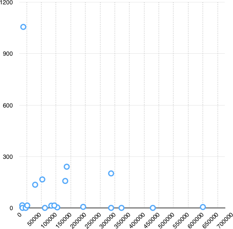
And another median:

This time the median value is 113 871 bits/s.
Reader max clock speed
Note that only 4 readers have a clock that can go up to 20 Mhz (or more). But I guess they are bogus readers.The highest "common" clock speed is more likely 16 Mhz with 16 readers (3.95%).